INFRA Signal 217
A 0.42-nanometer breakthrough could push transistors beyond silicon
 ↗
↗
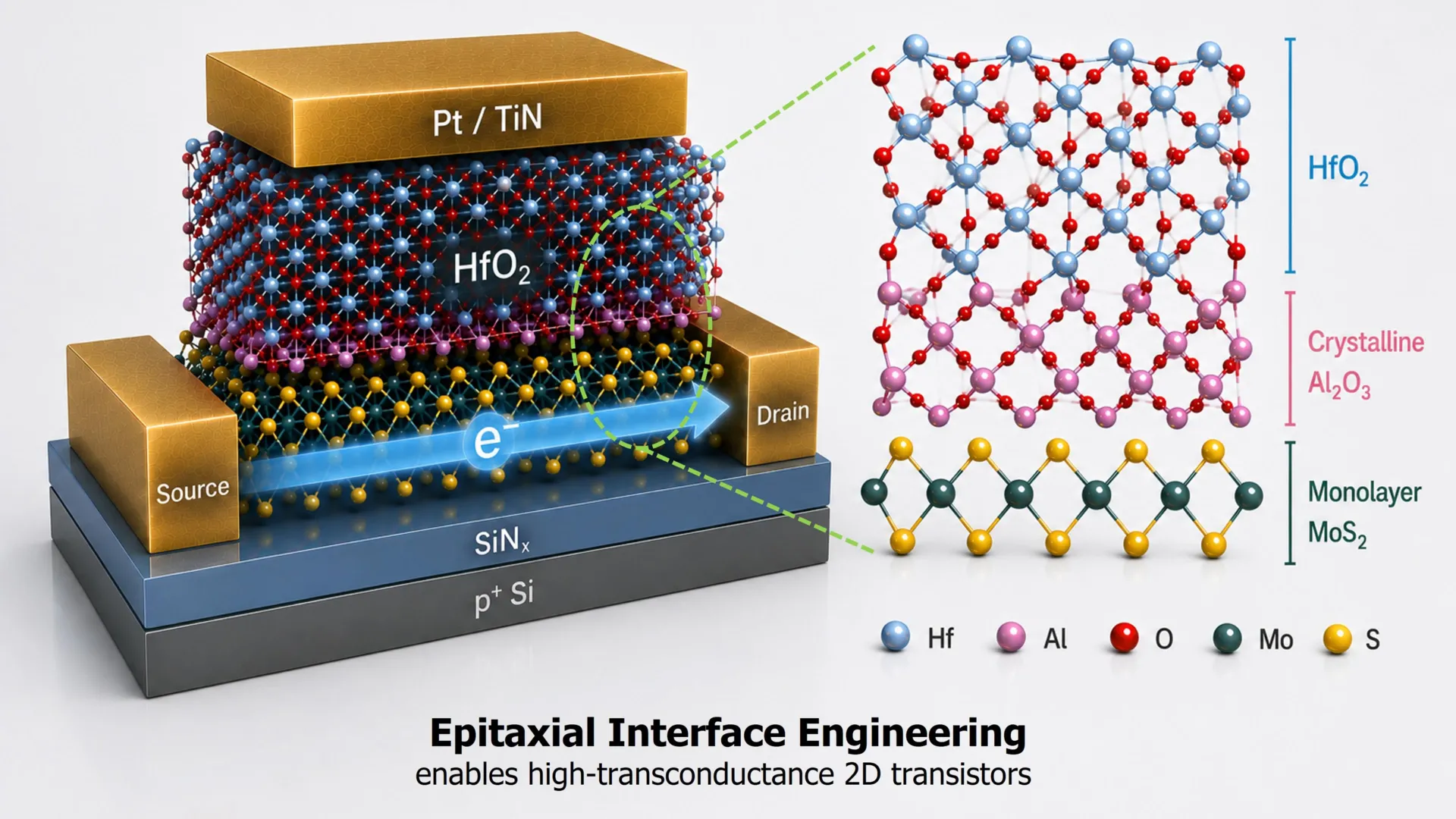
Researchers engineered a 0.42-nanometer aluminum oxide dielectric on monolayer MoS2 by oxidizing an epitaxial aluminum layer, breaking the tradeoff between gate control and carrier mobility that has limited 2D transistors.
For years, shrinking the gate dielectric on atomically thin semiconductors improved electrical control but disrupted electron flow at the material boundary. This work shows that engineering that boundary directly, rather than hunting for new semiconductor materials, can resolve the tradeoff, potentially making sub-silicon-scale transistors manufacturable.
Written by elseif from the cluster below · every claim links back to a sourceThe three things worth knowing
An ultrathin epitaxial aluminum layer was placed on monolayer MoS2 and then oxidized to form an aluminum oxide dielectric approximately 0.42 nanometers thick.
The approach targets the atomic interface between semiconductor and insulator rather than seeking new semiconductor materials.
The research was conducted by NYCU with TSMC Corporate Research and published in Nature Electronics.
THE CLUSTER