INFRA Signal 424
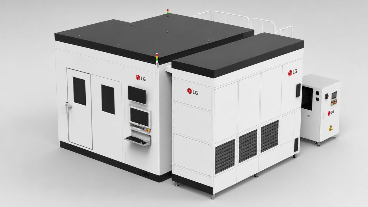
LG's maskless laser direct imaging tool targets chip packaging with 1.5-µm patterns
 ↗
↗
LG's production technology unit has signed a contract to supply a maskless laser direct imaging lithography tool for semiconductor packaging, capable of 1.5-µm line-and-space patterns.
For OSATs and packaging houses, this offers a maskless alternative to photomask-based lithography for patterning redistribution layers and high-density interconnects, with real-time pattern adjustment to compensate for substrate warpage. However, it cannot reach the resolution needed for CoWoS-S or CoWoS-L/EMIB, so it targets the RDL interposer tier and high-density PCBs.
Written by elseif from the cluster below · every claim links back to a sourceThe three things worth knowing
LG's LDI system uses a 405-nm laser diode and can process substrates up to 600×600 mm.
The maskless approach allows real-time pattern calibration to handle organic substrate expansion and warpage.
With 1.5-µm L/S capability, it targets RDL interposers and high-density PCBs, not the finest CoWoS nodes.
THE CLUSTER