DEV TOOLS Signal 56
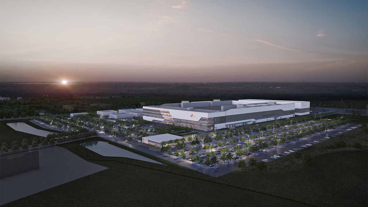
SK hynix launches construction of first US HBM packaging plant, targeting 2029
 ↗
↗
SK hynix held a groundbreaking for its Indiana HBM packaging plant, which will assemble HBM stacks from Korean DRAM wafers for U.S. AI customers, with production expected in 2029.
For engineers building AI systems, this plant shortens the iteration cycle for custom HBM designs by locating packaging and testing near U.S. customers. It also establishes an advanced packaging R&D testbed for prototyping and validation, which could accelerate adoption of customized HBM.
Written by elseif from the cluster below · every claim links back to a sourceThe three things worth knowing
The Indiana facility will specialize in advanced packaging, testing, and R&D of HBM, costing about $4 billion.
It will not manufacture DRAM wafers; it will package HBM stacks using DRAM wafers from South Korea and base dies from South Korea, Taiwan, or the U.S.
SK hynix expects to open the cleanroom by October 2028 and begin volume production in the second half of 2029, about a year later than originally planned.
THE CLUSTER